The best transistors in the world are now smaller than a strand of COVID virus. And yet, the more densely engineers pack them, the hotter chips run, the more energy they burn, and the worse the interference gets between adjacent components. The semiconductor industry has been wrestling with this for a decade, aware that pure miniaturization has an expiration date. AI made the deadline urgent. Training a frontier model today demands power that rivals a small city's consumption. Something in the physics has to give.
Key Insights You Should Never Miss
-
Light-Based Valley Computing.Valleytronics exploits the quantum valley degree of freedom in atomically thin materials to encode binary data via light chirality, successfully bypassing the thermal and interference limits of traditional electrical computing systems.
-
Room Temperature Operation Achieved.Unlike most quantum-adjacent technologies requiring extreme cooling, this newly integrated photonic chip operates stably at room temperature, making it a highly viable candidate for practical, real-world engineering applications.
-
Parallel Data Stream Processing.The chip successfully transmitted two independent images simultaneously through distinct valley-polarized pathways on a single device, proving the massive bandwidth and parallel processing potential of this new technology.
A research team at Monash University may have just pointed at what comes next. Their photonic valleytronic chip, published in Nature Photonics in May 2026, processes information using light rather than electrical current, and does so by exploiting a quantum property of certain crystalline materials that most people have never heard of: the valley degree of freedom. It is a small chip with a quiet publication and an implication that the computing industry has been circling for years without quite reaching.
What Valleys Are and Why They Matter for Computing
In certain atomically thin materials, like tungsten diselenide, electrons can occupy two distinct energy states that exist at opposite corners of the material's internal momentum structure. These states are called valleys. Think of them as two separate express lanes on a highway, each able to carry information independently without interfering with each other.
The clever part is the optical switch. Left-circularly polarized light excites electrons in one valley. Right-circularly polarized light excites the other. That gives researchers a clean, physically distinct way to encode binary data using the chirality of light itself rather than the flow of electrical charge.
Put that in a longer context and what becomes clear is that computing has historically added new degrees of freedom when old ones hit limits. Charge gave us classical electronics. Spin gave us a class of memory technologies. The valley degree of freedom is a third dimension of information encoding, one that operates through light and could, in principle, multiply what a chip can process per unit of material.
Why Integration Was the Barrier That Took Years to Break
Valleytronics has been theoretically compelling for well over a decade. The problem was practical. Laboratories could generate valley-polarized light signals in one experiment, route them in another, and detect them in a third. But each function required separate setups, different substrates, and equipment that would fill a room. A useful technology needs all three on one compact platform.
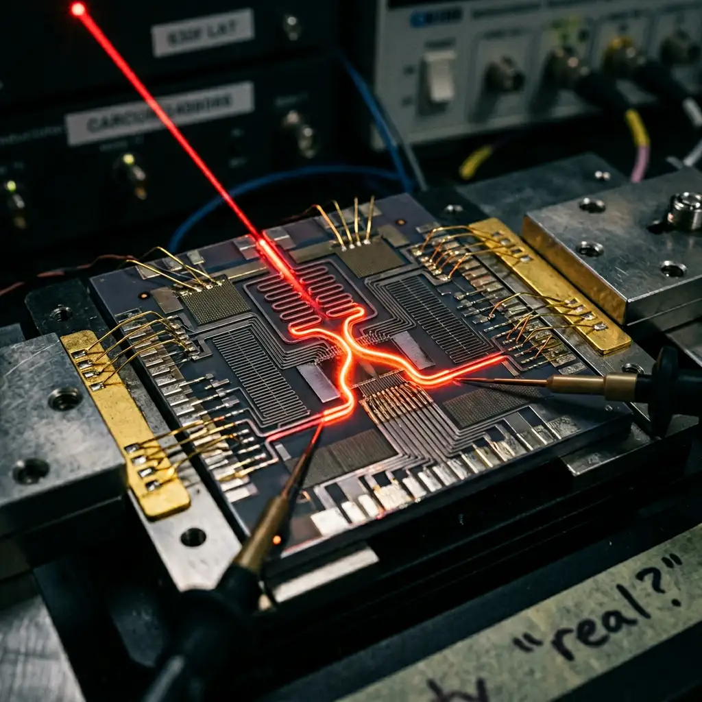
The Monash team solved it by designing what are called chirality-selective meta-waveguides: nanoscale patterned structures that capture and route photons based on their circular polarization. Paired with few-layer tungsten diselenide photodetectors, the result is a system that creates valley-encoded signals, steers them along programmable paths, and reads them out electrically, all within the same chip-sized device. The key engineering move was a stacking approach that integrates ultrathin materials with metasurfaces, sidestepping the extreme technical difficulty of growing those materials directly onto photonic structures.
What makes this more than a materials science curiosity is the operating temperature. Most quantum-adjacent technologies require cooling to near absolute zero, which makes them expensive, fragile, and impossible to deploy outside specialized facilities. This chip runs at room temperature. That one fact moves it from 'interesting physics' into the category of 'potential engineering foundation.'
In Simple Terms — The Valley Degree of Freedom
Think of a material's momentum structure like a highway with two separate, non-interfering express lanes. Electrons can occupy either lane, allowing data to be encoded and routed independently using light chirality, rather than traditional electrical charge.
Two Images, One Chip: The Proof That Valleys Can Carry Real Data
To validate what the system could actually do, the team encoded and transmitted two separate images through different valley channels on the same chip simultaneously. Each image traveled through a distinct valley-polarized pathway and was detected independently. The chip handled both at once.
This is worth pausing on. Parallel, independent data streams processed simultaneously on a single chip using quantum properties of light rather than electrical switching. Photonic systems can achieve massive bandwidths because photons do not generate heat or suffer the resistive losses that electrons do in metal wiring. The valley multiplexing demonstrated here adds another layer: different information can travel in different valley states through the same physical channel, which is closer in principle to how fiber-optic wavelength division multiplexing works than to how a conventional processor routes data.
What has not been published yet are benchmarks. The team has not released data on bit rates, signal-to-noise ratios, or energy consumed per operation. The demonstration proves functional integration, not commercial-grade performance. That distinction matters, and honest assessment requires holding it.
Where Valleytronics Fits in the Photonic Computing Landscape
Silicon photonics is already deployed at scale in data centers, replacing electrical chip-to-chip links with optical ones. Companies including Nvidia have made substantial investments in photonic interconnect firms, driven by the simple reality that AI models with hundreds of billions of parameters move more data between components than copper wiring can physically handle.
But silicon photonics largely replaces wire with light. It is a faster pipe. The valleytronic approach is different in kind: it encodes and processes information using quantum properties of the light itself. This does not compete with silicon photonics so much as it proposes a layer above it, where light is not just a transport medium but a computational substrate. Valley states have also been proposed as carriers of quantum information, which means the same material platform could, in the long run, serve both classical photonic acceleration and early quantum processing. That intersection is where the long-term interest lies.
The Hard Road from Lab Circuit to Working Technology
The current device processes two channels. A commercially relevant system would need to handle thousands. Stacking atomically thin materials with metasurfaces is a painstaking laboratory process with no established path to high-volume manufacturing. The excitonic states that enable valley polarization also have relatively short lifetimes, which poses questions about stability during extended operation.
The history of optical computing is not encouraging. Earlier generations of photonic computing research produced promising demonstrations across multiple decades without ever producing a product that competed with silicon. That history is a real constraint on how confidently anyone should project a roadmap from this chip.
What has changed is the material and fabrication toolkit. Two-dimensional materials like tungsten diselenide, precision nanofabrication at scales below 10 nanometers, and the ability to integrate dissimilar materials through stacking rather than growth -- none of these were available to researchers who made similar theoretical arguments twenty years ago. The current moment is genuinely different, even if the destination remains uncertain.
In Simple Terms — Chirality-Selective Meta-Waveguides
These are nanoscale patterned structures that act like specialized traffic controllers for light. They capture and route photons based specifically on their circular polarization, enabling the chip to steer distinct data streams without them mixing or interfering.
A Third Degree of Freedom Could Change What Computing Means
The transistor was demonstrated in 1947. It took over a decade to appear in commercial electronics. The gap between 'we proved this works' and 'this works at scale in the world' is where most laboratory achievements disappear.
What the Monash team has done is cross the integration threshold that valleytronics has been stuck behind. A chip that generates, routes, and detects valley-encoded optical signals in a single device, at room temperature, processing multiple independent streams simultaneously -- that is a first. Whether it becomes a foundation or a footnote depends on whether the fabrication can be industrialized, whether the performance benchmarks hold up, and whether the economics ever compete with silicon.
The physics works. The room-temperature operation works. The integration works. What nobody knows yet is whether this can be made to work at the speed, the yield, and the cost that separates a laboratory achievement from something that actually runs in a server rack.
That question will take years to answer. But the question itself is new. Until this chip existed, it could not even be properly asked.