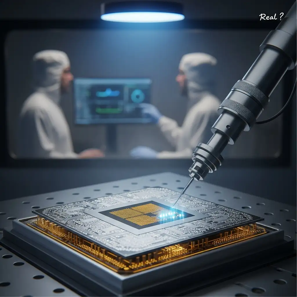
A data center running a single large AI model can pull enough electricity to power a small town, and most of that power disappears as heat before it ever produces a useful answer. That is the quiet math behind every AI headline this year. Chips keep getting more capable, but the energy bill keeps climbing faster than most people notice.
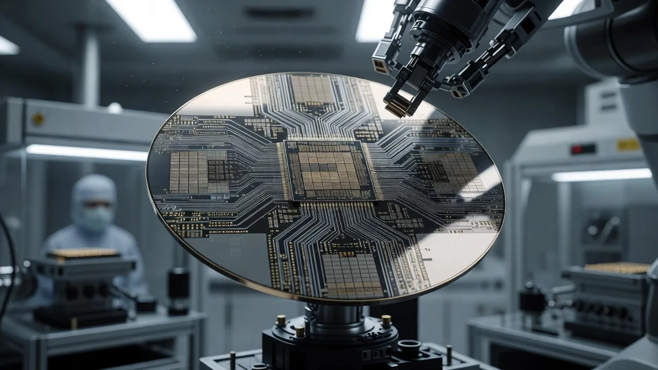
AI Generated Illustration
IBM's newest transistor architecture, reported at a physical scale near 0.7nm, is not really a story about a number. It is a story about engineers running out of room to shrink things and choosing to redesign the transistor itself instead. That distinction matters more than it sounds, because the entire history of computing progress has quietly depended on transistors getting smaller every couple of years. When that stops working, something else has to take over.
This is where the deeper question sits. If shrinking transistors is no longer the main lever for progress, what exactly did IBM change, and can it actually keep computing moving forward the way smaller transistors used to?
Why Conventional Chip Scaling Is Reaching Its Limits
For roughly fifty years, semiconductor progress followed a simple pattern known as Moore's Law: pack more transistors into the same space, and chips get faster and cheaper almost automatically. That pattern held up remarkably well, largely because transistors could keep shrinking without breaking the physics that made them work.
That is no longer true. At today's scale, transistors are so small that electrons start leaking through barriers that used to block them completely, a problem engineers call power leakage. Heat builds up faster than it can escape, and manufacturing chips at this scale requires machines and materials so precise that a single fabrication plant can cost tens of billions of dollars to build.
None of this means engineers gave up on progress. It means the strategy changed. Instead of asking how much smaller a transistor can get, chipmakers started asking how a transistor is built in the first place, down to its shape, its materials, and how current physically moves through it.
How IBM Reinvented Transistor Architecture
IBM's approach centers on restructuring the transistor rather than simply compressing it. Traditional transistors sit flat on a chip's surface, side by side, wasting a lot of the surface area between them. IBM's design stacks transistor components vertically instead, similar to how a city solves a housing shortage by building upward instead of spreading further out. More useful structure fits into the same footprint, and current has a shorter, more efficient path to travel.
The 0.7nm figure being widely discussed represents a research-stage demonstration, not a chip you would find in a laptop next year. Commercial node names like 3nm or 2nm have described marketing categories rather than literal transistor measurements for years now, so a lab result at this scale signals direction more than it guarantees a specific product timeline.
What IBM has published so far emphasizes efficiency potential rather than a full performance profile. Real-world numbers on speed, yield, and heat under sustained workloads have not been disclosed in detail, which means the promising part of this story still needs to be proven outside a research lab.
Why This Could Change AI Computing More Than Consumer Devices
A smartphone chip mostly needs to be fast enough for what a person notices, scrolling, opening apps, running a camera. AI infrastructure runs a different kind of workload entirely: massive clusters of chips training and running models around the clock, where even a small efficiency gain multiplied across thousands of processors turns into a real difference in electricity and cooling costs.
This is why lower power consumption may matter more here than raw speed. AI accelerators, cloud servers, and edge devices that run inference locally all share the same constraint, which is that power draw limits how much computing they can pack into a given space before heat becomes the bottleneck rather than the chip design itself.
There is a sharper way to put it. The next era of AI leadership may not be decided by whose chip runs the fastest benchmark, but by whose chip does the most useful work per watt of electricity it burns. Speed used to be the scoreboard. Efficiency is becoming the scoreboard now, and that shift changes which companies actually have the advantage.
The Race Beyond Moore's Law Is Accelerating
IBM is not working on this in isolation. Across the semiconductor industry, companies are pursuing several parallel strategies at once: new transistor geometries like the one IBM is developing, advanced chip packaging that stacks multiple chiplets together instead of relying on one giant chip, and backside power delivery, which reroutes a chip's power wiring to the back of the silicon to free up more room on the front for actual computing.
None of these approaches is being treated as the single answer. That is deliberate. Betting everything on one breakthrough is risky when the physics keeps shifting, so companies are hedging by advancing multiple technologies simultaneously and letting whichever combination proves most manufacturable win out.
That word, manufacturable, is doing a lot of quiet work here. A brilliant transistor design that cannot be built reliably at scale is a research paper, not a product. Which raises the harder question underneath all of this.
What Could Slow the Journey From Lab to Commercial Chips
Getting a new transistor architecture from a research demonstration into billions of shipped chips is where most breakthroughs actually die, not in the lab. Fabrication at this scale demands extraordinary precision, and even a small drop in production yield, the percentage of chips that come off the line actually working, can make a design too expensive to sell.
Equipment costs alone can stall progress for years. The specialized machines needed to manufacture next-generation transistors take enormous capital investment and long lead times to install, and supply chains for the materials involved are neither simple nor guaranteed to stay stable.
What remains unclear is how long the gap will be between IBM's lab result and an actual chip built on this architecture reaching a data center. History suggests that gap tends to run longer than early announcements imply, and engineering feasibility and manufacturing economics, not laboratory performance alone, ultimately decide whether a design like this ever ships.
What This Breakthrough Could Mean for the Future of Computing
What IBM's research really signals is a shift in what counts as progress. For decades, smaller meant better, almost by definition. Now the industry is quietly redefining better as smarter architecture and lower energy use, even if the transistor stops shrinking much further.
The long-term stakes reach well past any single chip. AI research, scientific computing, and everyday consumer devices all depend on hardware that can do more without demanding more electricity from a grid that is already strained by other pressures. A transistor design that meaningfully cuts power use touches all of it at once, not just one product category.
The next era of computing may end up being defined less by who builds the smallest transistor and more by who delivers the most computing power for the least energy spent doing it. Whether IBM's specific design becomes the one that gets there, or simply pushes competitors toward their own version of the same idea, is the part nobody can answer yet.