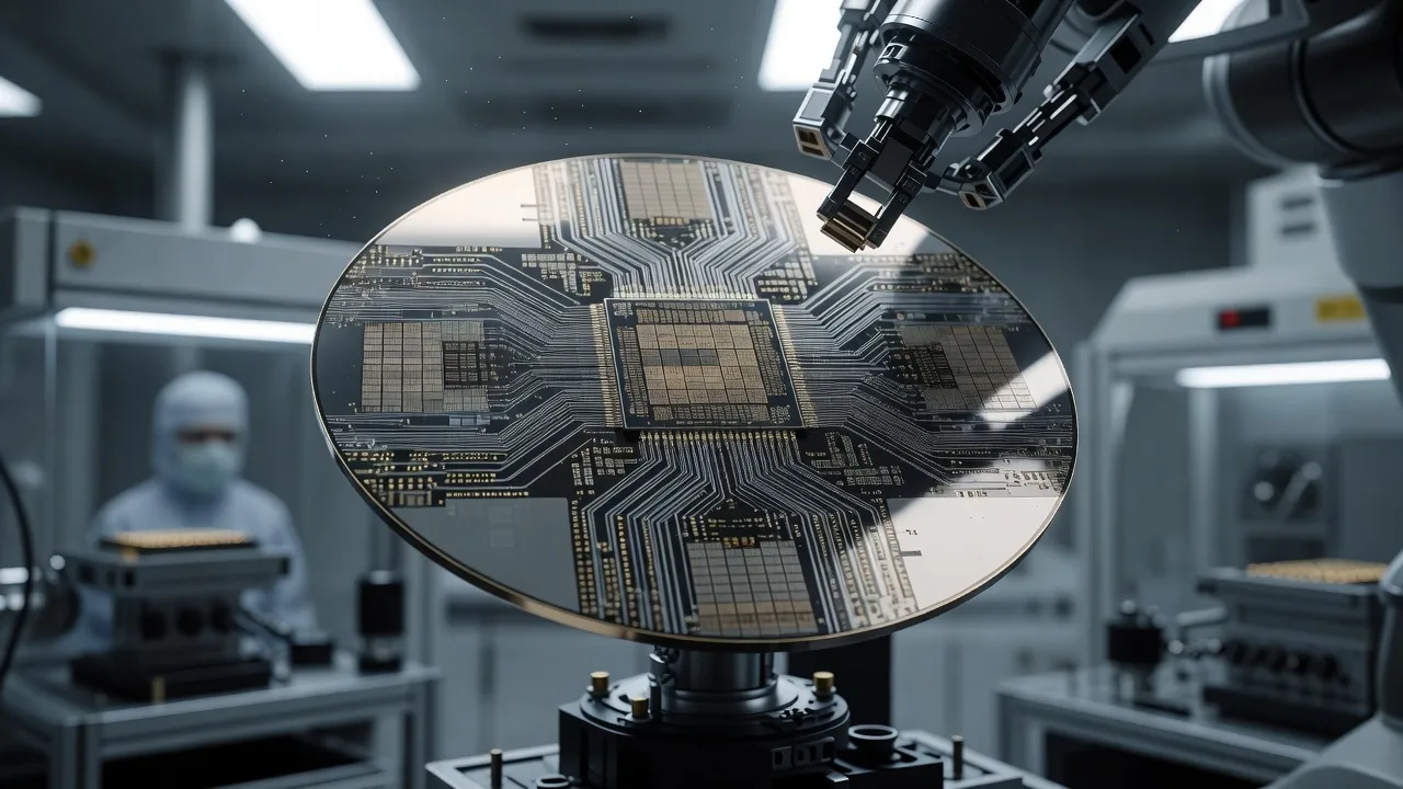
A new number is making the rounds in chip research: 0.42 nanometers, about the thickness of two atoms stacked together. It sounds like a breakthrough that shrinks your next laptop's processor to something almost inconceivably small. It doesn't, and what that number actually describes turns out to be more interesting than the headline itself. The 0.42-nanometer figure belongs to an ultrathin aluminum oxide interface, not a processor, not a chip, and not a manufacturing node you'll ever see on a spec sheet.
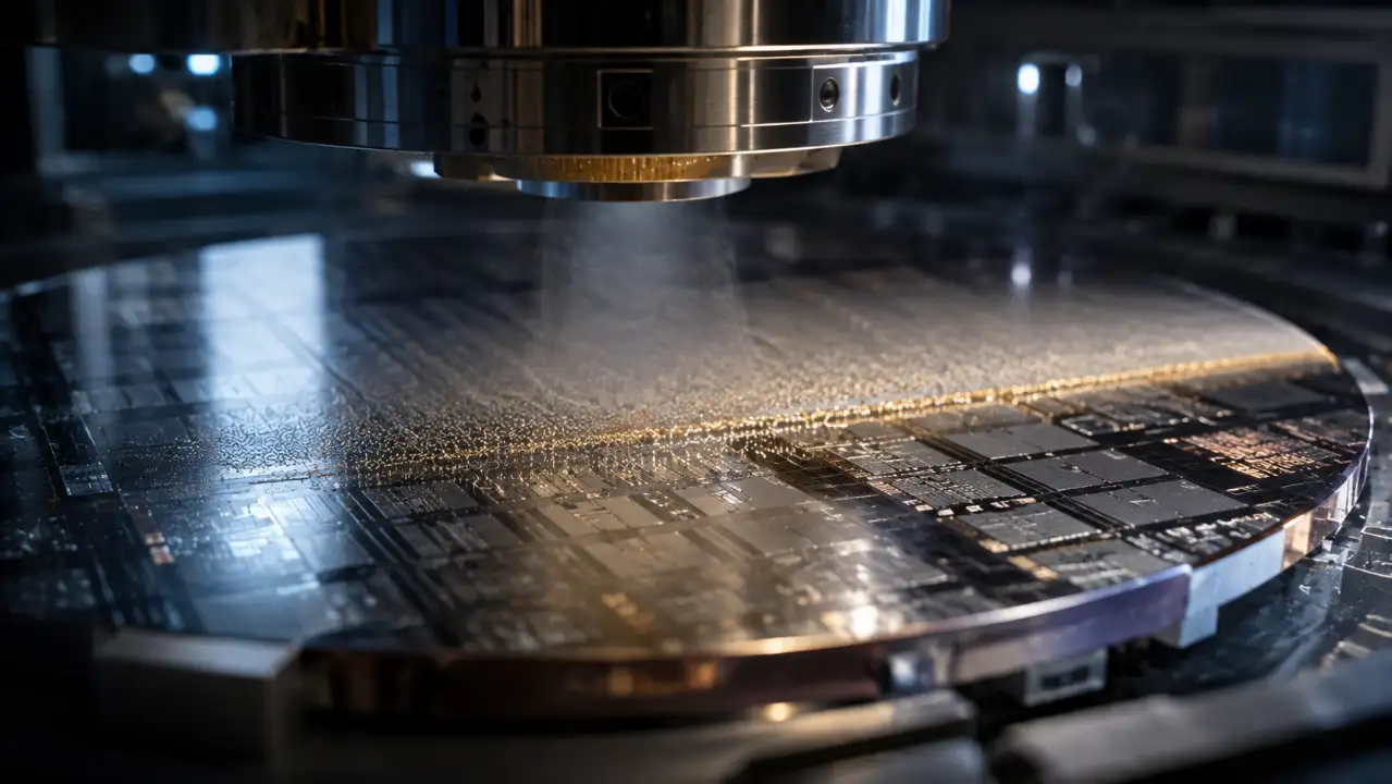
AI Generated Illustration
The interface sits inside an experimental transistor built around monolayer MoS₂, one of a class of materials called 2D semiconductors, so named because they can exist as a layer only a single atom thick. Researchers have been chasing materials like this because silicon chips are running into physical limits that are getting harder to engineer around, and a channel that thin offers a way to keep shrinking transistors without losing the electrical properties that make them work. That's the real appeal here. This isn't a faster consumer chip. It's a possible way to keep making transistors smaller once silicon runs out of room.
The distinction matters because the interesting part of this study isn't the number itself. It's what a two-atom-thick layer of aluminum oxide is doing for a transistor built from an entirely different material. Getting that boundary right turns out to be one of the more stubborn problems standing between 2D semiconductors and real chips, and the number now circulating in headlines is really a byproduct of solving it.
Before getting into how the researchers pulled this off, it helps to understand why the interface was the problem in the first place.
The Real Problem Is Happening Between Materials
Every transistor needs a gate dielectric, a thin insulating layer that sits between the gate electrode and the semiconductor channel. Thinner dielectrics let the gate exert stronger control over the channel, switching the transistor on and off more precisely, which is one of the main levers engineers pull to make transistors smaller and more efficient.
The trouble shows up when that dielectric touches something as thin as monolayer MoS₂. Conventional gate materials placed directly against a single layer of atoms tend to introduce defects and rough interactions at the boundary, scattering the electrons trying to move through the channel and dragging down performance. Thinning the gate helps the transistor's control, but it risks damaging the very property that made the thin channel worth using in the first place.
That tension between tighter control and preserved electron flow is the central engineering problem in this corner of chip research. Instead of chasing a better semiconductor material outright, the team behind this work went after the boundary between the materials themselves.
How Two Atomic Layers Change the Transistor
The approach was to deposit a thin layer of aluminum directly onto monolayer MoS₂ and then oxidize it, producing a crystalline aluminum oxide layer roughly 0.42 nanometers thick, about two atoms deep. That layer doesn't replace the transistor's main gate dielectric. It sits underneath it, acting as a buffer between the delicate MoS₂ channel and the high-k hafnium oxide dielectric placed on top.
Think of it less like insulation and more like a gasket, a precisely fitted layer that lets two surfaces meet without damaging either one. The aluminum oxide gives the hafnium oxide a clean, stable surface to grow on, while shielding the MoS₂ underneath from the kind of atomic-scale roughness that normally hurts performance.
The reported results back up the idea that the fix worked. The team measured a peak transconductance of about 0.45 milliSiemens per micrometer, a way of describing how effectively the gate voltage controls current through the channel, alongside an equivalent oxide thickness of about 1 nanometer, a measure of how thin the effective dielectric behaves electrically. Both numbers point toward a transistor that switches efficiently without sacrificing the channel's electrical quality.
At this scale, the interface stops being a minor detail sitting around the transistor. It becomes part of the transistor's actual performance, which raises the question of why anyone would bother with a material like MoS₂ in the first place.
Why MoS₂ Could Matter After Silicon
Silicon transistors have been shrinking for decades, but the dimensions involved are approaching limits where making the channel any thinner starts to hurt more than it helps. Chipmakers have compensated with increasingly elaborate three-dimensional architectures, stacking and folding silicon structures to keep gaining density even as flat scaling runs out of headroom.
A material like MoS₂ sidesteps part of that problem because its natural form is already close to the physical limit. A channel that's one atomic layer thick doesn't need the complicated engineering that silicon requires to behave the same way, which is the basic argument researchers make for pursuing 2D semiconductors as a long-term direction rather than a short-term fix.
None of this means silicon is going anywhere. Beyond silicon doesn't mean silicon suddenly stops working in the billions of chips already built around it. The more accurate way to think about this research is as an early step toward a new material and device platform that could eventually complement silicon logic in specific applications, not replace the entire foundation of the semiconductor industry overnight.
That framing matters, because it's exactly where a lot of the public confusion about announcements like this one tends to start.
The 0.42-Nanometer Layer Does Not Mean 0.42-Nanometer Chips
It's worth saying plainly: this is not a sub-1-nanometer chip, and there is no new 0.42-nanometer manufacturing node on the horizon. Modern chip node names, things like 3-nanometer or 2-nanometer processes, haven't corresponded to a single physical measurement for years now. They function more as marketing shorthand than literal descriptions of feature size, and the 0.42-nanometer figure from this research describes one interface layer inside an experimental device, not a full manufacturing standard.
The transconductance and equivalent oxide thickness numbers are genuinely promising for a lab-built transistor, but they don't establish anything about processor-level speed, power draw, chip density, manufacturing yield, or whether this approach could compete commercially with existing silicon processes. Those questions sit well outside what a single transistor measurement can answer.
That gap between what was demonstrated and what gets implied by a headline is exactly why it's worth separating the two. The real achievement here is narrowing a specific transistor-level bottleneck, not shipping a finished next-generation chip, and the difference between those two things is where the much larger challenge begins.
The Hardest Part Comes After the Laboratory
Getting one transistor to work well on a bench is a different problem than manufacturing billions of identical ones across a silicon wafer. Wafer-scale growth of monolayer MoS₂, precise integration with other materials, reliable electrical contacts, defect control, and process uniformity all have to work at once, and each one carries its own open research questions.
A transistor architecture has to perform consistently across enormous numbers of devices before it has any chance of appearing inside a CPU, GPU, or AI accelerator. Semiconductor manufacturing runs on repeatability at a scale that laboratory demonstrations rarely have to account for, and that gap has stalled plenty of promising materials before they ever reached a production line.
So it's fair to read this result as reducing one real technical risk on a possible path beyond silicon, rather than proof that the path is clear. The physics working in a lab is one hurdle. Making it work the same way across an entire fab, at industrial volume, is a much longer and far less forgiving one.
A Possible New Route to Smaller, More Efficient Chips
If interface engineering like this keeps improving, it could support future transistors with tighter electrostatic control, opening room for continued scaling and better energy efficiency at a point where silicon alone is struggling to deliver either. That matters most for workloads like AI accelerators, where transistor density and power consumption are already pressing against real limits.
The immediate significance of this research isn't a faster phone next year. It's evidence that one of the specific obstacles holding back atomically thin semiconductors, the messy boundary where two materials meet, can actually be engineered around rather than just worked around.
Chip scaling has spent fifty years being mostly a story about making silicon smaller. This result raises a quieter question: what happens once the more interesting engineering problem stops being how small you can make the material, and becomes how precisely you can control the seam where two materials meet?